ASML: Exclusive Interview for AT
This is one of the most eagerly awaited interviews on my part. On the one hand because it is about the semiconductor sector, and on the other hand because it is one of the two jewels of Europe in terms of technology, along with IMEC. This is the company ASML, a world leader in chip manufacturing equipment, such as photolithography machines.
If you want to know more about this exciting sector and about the company itself, you should read this company’s interview…

Architecnología: IMEC and ASML are the European jewels of technology. What is the relationship between IMEC and ASML based on? Is the collaboration unidirectional or bidirectional?
ASML: Imec is a very important research partner for ASML as well as for the entire semiconductor industry. We have been collaborating closely with them for many years. It is a bidirectional collaboration, which is the strength of this partnership. Imec is the place where the semiconductor industry collaborates on pre-competitive research. .
AT: And with foundries? I mean once ASML sells the productos to the fab, Does any service beyond technical support? For example, Is there any kind of feedbak to improvement the products?
ASML: Our customers are foundries but also companies like Intel. Our customers are all of the world’s leading chip manufacturers. We work closely with them to ensure we understand their needs, priorities and challenges.
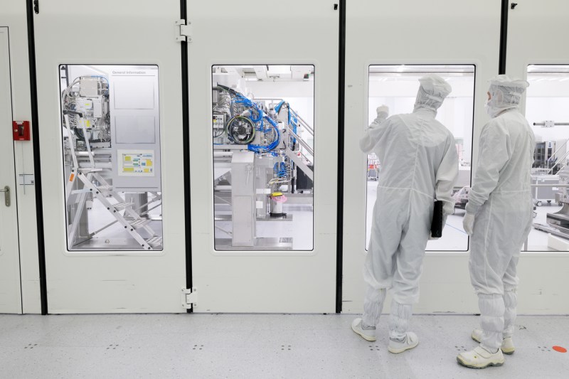
We have a customer support group that services our systems in the field, in the customers’ fabs. They install the systems, service them and upgrade (software or hardware) when needed/requested. We are in our customers’ fabs every day.
We have a very close relationship with our customers. Our success is inextricably linked with our customers’ success. For this reason, we engage with our customers at all levels: building partnerships, sharing knowledge and aligning our investments in innovation. We design our machines based on their input, engage in helping them achieve their technology and cost roadmaps, and work together, often literally in the same team, to make sure our machines are running smoothly in their fabrication plants (fabs).
AT: Why is the demand for DUV systems still so high? Is it due to the complexity of EUV or is there something else?
ASML: DUV is the workhorse of the semiconductor industry. The technology is used to produce chips that are used everywhere. EUV is for the advanced nodes which are not required for every chip, only the high-end, most complex chips (and within that chip, the most complex layers). So DUV is and will remain important and the demand continues to be high. With the introduction of EUV, more advanced chips can be made fast and in a cost effective way. But still, even with these chips, DUV plays an important role in the less complex layers (each chip consists of layers which are built on top of each other in a process in the fab which requires many different types of equipment – not only lithography (DUV/EUV). See our website: How microchips are made | ASML.

AT: What are the main optical challenges you are facing given the tiny dimensions you are working with?
ASML: The main optical challenges are twofold. Firstly, the optical design has very strict requirements, especially for EUV. For example, the mirrors that are used in an EUV system have to be atomically flat, with a tolerance of picometer. This requires the world’s best polishing techniques and measurement techniques, which are ZEISS’ expertise. Secondly, due to the heat of the light that the guide through our systems, the optics tends to deform, negatively impacting the resulting image. We need to correct for that in real-time, both through sensors and actuators in the mirrors, and through advanced software models.
AT: Why Zeiss as a lens supplier? Do they provide any competitive advantage over other optical suppliers?
ASML: Zeiss produces the optics in our systems, the lenses and mirrors. They are the only supplier that can develop and manufacture the quality that we need. They are truly unique and the partnership with ASML is exclusive, it is a very tight collaboration in every way.

AT: How do you see the EU boost to the European semiconductor industry? Have you noticed an increasing demand for equipment as a result?
ASML: It is too soon to see a boost in demand as a result of the EU plans for the semiconductor industry. If you look at our sales per region, you see that the vast majority of our systems go to Asia. Q3 2021 System sales per region (and full year 2020):
- South Korea: 33% (31%)
- Taiwan: 46 (36%)
- China: 10% (18%)
- Japan: 1% (3%)
- US: 10% (9%)
- EMEA: – (2%)
AT: The semiconductor industry consumes a lot of electrical energy and also water. How are you working from ASML to reduce the consumption of your equipment? Do you have numbers to prove the progress?
ASML: Yes .We drive a roadmap towards zero waste by 2030 and net zero value chain emissions by 2040. We are updating our ESG Sustainability policy which will be published in our Annual Report in February 2022. This is the slide that our CEO Peter Wennink presented during the Investor Day in September:

AT: After µm and nm, we are now talking about Å. Single Si atoms have a size around 0.2nm (2Å). What is the real limit of silicon-based technology? Would it be possible to create circuits with single atom wide devices or would their behavior be unstable and complicated to control?
ASML: I You should take this question to the world’s top chipmakers.
AT: Which will be reached first? The limit of dimensions or the limit of power?
ASML: The chip industry is a creative powerhouse that has been finding solutions to challenges for over 60 years. The real question is not whether a chip structure can be made, but whether it can be mass produced in an affordable way. We have a roadmap in place to continue scaling and mass production for the next decade, and are working with our customers to make it happen.

AT: Once this limit is reached ¿what? Do you have a rough estimate of when this inflection point will be reached?
ASML: Based on the roadmaps of our customers, we see Moore’s Law continuing for the next decade, and especially in terms of system scaling (integration of chips, new architectures, new materials, power reductions, etc), our customers are extremely bullish on the innovation that is ahead.
AT: Now MESO (MagnetoElectric Spin-Orbit) technology has been mentioned as a beyond-CMOS solution. Are you working on the development of future equipment for this new era?
ASML: We are always in touch with our customers on what they need for the future.
AT: Finally, Can your photolithography equipment work on any type of fab (MEMS, SiC based electronics, solar cells…)?
ASML: Yes. Our lithography systems are built with modularity in mind, so they can be tweaked to fit a customer’s process.